Open-source EDA · Building cimeda
Building cimeda:
an open-source workbench for IC design.
Bringing schematics, simulation and layout into one place—and looking for co-founders to build it with me.
Open-source EDAIC designBuilding cimeda
cimeda on GitHub ↗Currently private
Why I care about open-source EDA
Designing a chip means moving between a circuit idea, a schematic, simulations and a physical layout. For my work on AI hardware, I want that loop to be easier to explore, inspect and repeat.
Open-source electronic design automation (EDA) gives us a strong foundation. Projects such as Xschem for schematics and ngspice for circuit simulation already do essential work. I’m interested in how we connect those tools into an environment that feels coherent, while keeping designs and results accessible.
Meet cimeda
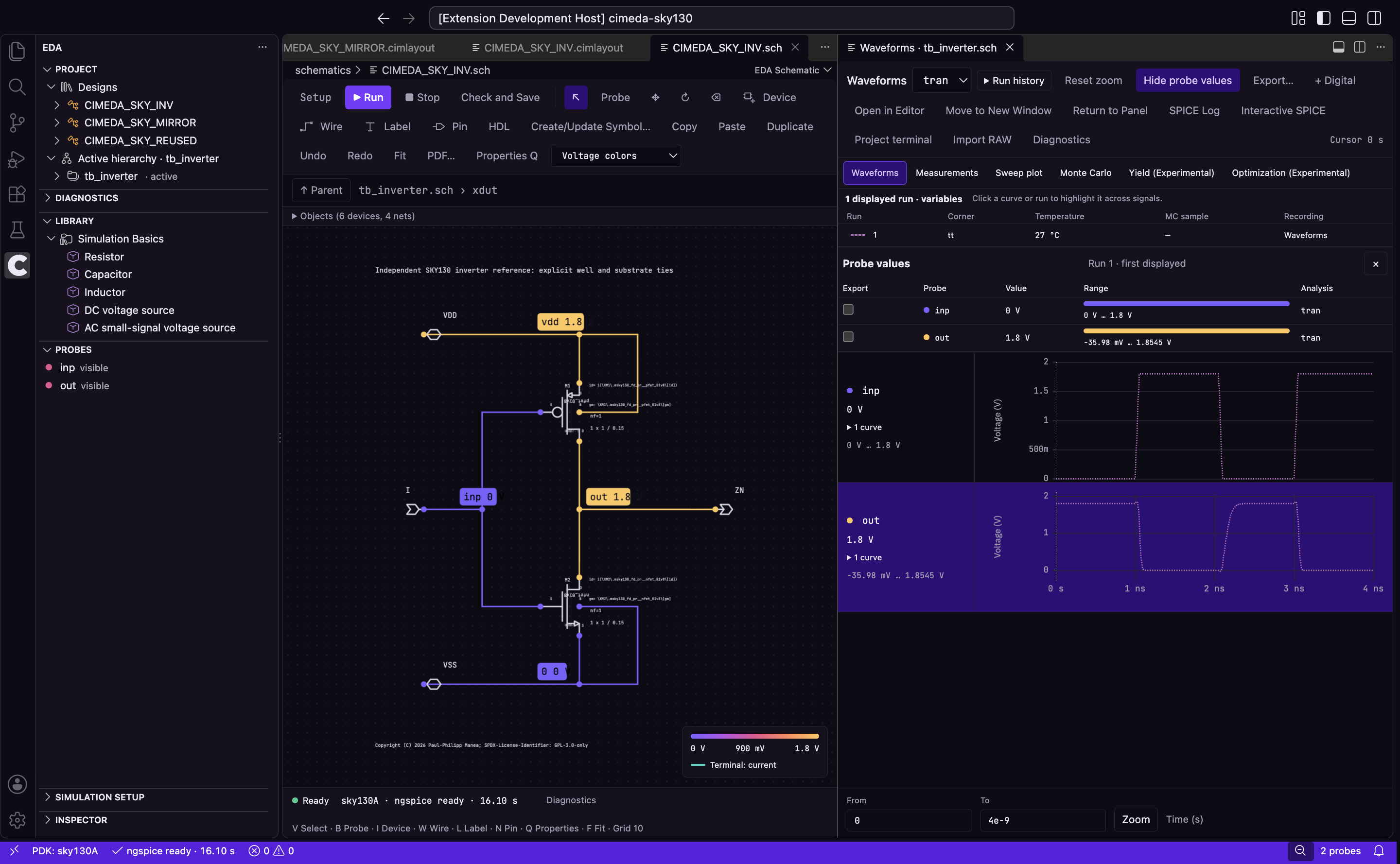
I’m building cimeda, an open-source workbench for integrated-circuit design. It brings schematic editing, simulation, waveform analysis and IC layout into an editor-based workspace. The shared extension runs in VS Code, VSCodium and the cimeda-branded application.
The project uses GPL-3.0-only licensing and builds on open-source EDA tools. Its analog workflows support the GF180MCU and SkyWater SKY130 process design kits—the device models and process information needed to design for a particular technology.
- Draw and reuse circuits. Work with native Xschem schematics, hierarchy, symbols and associated testbenches.
- Run and understand experiments. Use ngspice analyses, parameter sweeps, process corners and Monte Carlo studies, then inspect waveforms and measurements together.
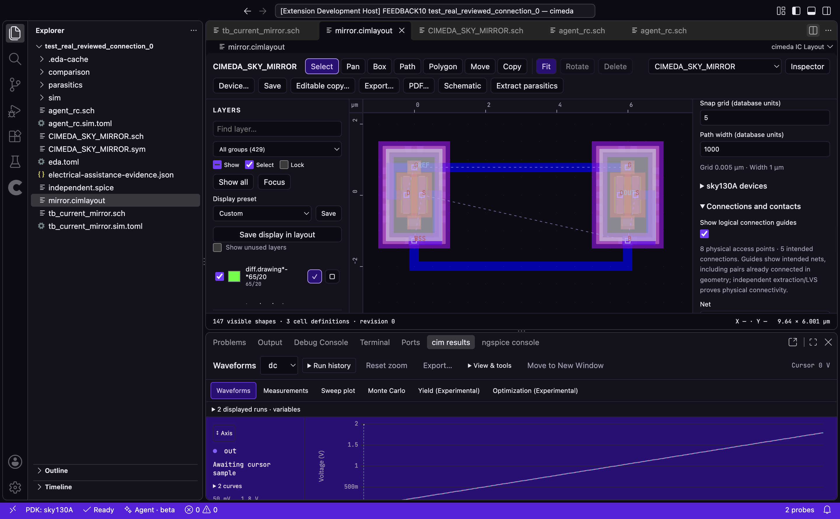
- Connect circuits to layout. Explore IC geometry, select related schematic and layout devices, and use Magic/Netgen checks. Experimental parasitic extraction helps compare ideal and extracted circuit behaviour.
Where AI fits
I’m also exploring AI-assisted IC design. The current agent beta connects compatible tools such as Claude Code or Codex through MCP, giving an agent access to schematic context, testbenches and numerical results. Proposed edits can be reviewed, applied with Undo and saved explicitly.
The goal is to make experiments easier to set up and understand while keeping the engineer involved in design decisions. This is active development: layout authoring is alpha, agent integration is beta, and generated circuits still need electrical and physical verification.
What I’ll write about next
I’ll use this blog to share practical notes on open-source EDA, circuit simulation and building cimeda: what works, what needs work, and what I learn along the way.
Project details and original screenshots are drawn from the cimeda development repository’s README and recorded application captures. Explore the upstream projects: Xschem and ngspice.